Full Adder Circuit Diagram In Verilog
Verilog adder example fulladder below gates exercises basis form will Understanding fpga programming and design flow Verilog code for full adder
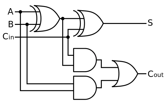
Full Adder : Circuit Diagram, Truth Table, Equations & Verilog Code
Verilog full adder example Adder circuit diagram basic gates using truth table Adder verilog code flow core fpga understanding programming figure
Adder datasheet
Verilog code for full adder using behavioral modelingDesign a serial adder circuit using verilog Adder verilog behavioral logic truth cout technobyteAdder verilog.
Verilog adder code structural using behavioral project implemented bothFull adder : circuit diagram, truth table, equations & verilog code Cd4008 4-bit full adder ic pinout, working, example and datasheet.


Verilog Full Adder example
CD4008 4-Bit Full ADDER IC pinout, working, example and datasheet

Understanding FPGA Programming and Design Flow - HardwareBee

Design a serial adder circuit using Verilog

Verilog code for Full Adder - FPGA4student.com

Full Adder : Circuit Diagram, Truth Table, Equations & Verilog Code
